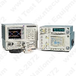
Tektronix BSA125C
BSA125C BERTScope 12.5 Gb/s Bit Error Ratio Analyzer
Description
The BERTScope Bit Error Rate Tester Series provides a new approach to signal integrity measurements of serial data systems. Perform bit error rate detection more quickly, accurately, and thoroughly by bridging eye diagram analysis with BER pattern generation. The BERTScope Bit Error Rate Tester Series enable you to easily isolate problematic bit and pattern sequences, then analyze further with advanced error analysis that deliver unprecedented statistical measurement depth.
Key performance specifications
- Pattern Generation and Error Analysis, High-speed BER Measurements up to 12.5 Gb/s
- Fast Input Rise Time / High Input Bandwidth Error Detector for Accurate Signal Integrity Analysis
- Physical Layer Test Suite with Mask Testing, Jitter Peak, BER Contour, and Q-factor Analysis for Comprehensive Testing with Standard or User-defined Libraries of Jitter Tolerance Templates
- Integrated Eye Diagram Analysis with BER Correlation
- Optional Jitter Map Comprehensive Jitter Decomposition - with Long Pattern (i.e. PRBS-31) Jitter
- Patented Error Location Analysis™ enables Rapid Understanding of your BER Performance Limitations and Assess Deterministic versus Random Errors, Perform Detailed Pattern-dependent Error Analysis, Perform Error Burst Analysis, or Error-free Interval Analysis
Key features
- Integrated, calibrated stress generation to address the stressed receiver sensitivity and clock recovery jitter tolerance test requirements for a wide range of standards
- Sinusoidal jitter to 100 MHz
- Random jitter
- Bounded, uncorrelated jitter
- Sinusoidal interference
- Spread spectrum clocking
- PCIe 2.0 & 3.0 receiver testing
- F/2 jitter generation for 8xFC and 10GBASE-KR testing
- IEEE802.3ba & 32G fibre channel testing
- Electrical stressed eye testing for
- PCI express
- 10/40/100 Gb Ethernet
- SFP+/SFI
- OIF/CEI
- Fibre channel (FC8, FC16, FC32)
- SATA
- USB 3.1
- InfiniBand (SDR, QDR, FDR, EDR)
- Tolerance compliance template testing with margin testing
- Integrated eye diagram analysis with BER correlation
Applications
- Design verification including signal integrity, jitter, and timing analysis
- Design characterization for high-speed, sophisticated designs
- Certification testing of serial data streams and high performance Networking systems
- Design/Verification of high-speed I/O components and systems
- Signal integrity analysis – mask testing, jitter peak, BER contour, jitter map, and q-factor analysis
- Design/Verification of optical transceivers
Features |
Benefits |
| Pattern Generation and Error Analysis, highspeed BER Measurements up to 12.5 Gb/sec. | The combination of impairment modulation, signal generation and analysis in one instrument enables receiver BER compliance testing for today's 3rd Generation Serial and 100G standards like; IEEE802.3ba, OIF-CEI and 32GFC communications standards. |
| Integrated Stress Generator for stressed eye sensitivity (SRS) and jitter tolerance compliance testing. | A test signal's data rate, applied stress, and data pattern can be changed on the fly, independent of each other; enabling a diverse set of signal variations for testing chipset/system sensitivity. |
| Integrated, BER correlated eye diagram analysis with pass/fail masks for PCI Express, USB, SATA and other communications standards. | Enhances the debug experience unlike other BERT's by providing a familiar eye diagram of the test results to compare against a standards specific mask. |
| Error Location and BER contour analysis on PRBS 31 and other digital signals up to 12.5 Gb/sec. | Provides a quick understanding of signal integrity in terms of BER. Error location provides detailed BER pattern sensitivities to speed up identification of deterministic vs. random BER errors. |
| Optional Jitter Map provides fast jitter decomposition, accurate stress calibration at the DUT input. | Fast, effective method |
- Data rate range
-
- BSA125C
- 0.1 to 12.5 Gb/s
- Format
- NRZ
- Polarity
- Normal or inverted
- Variable cross over
- 25 to 75%
- Patterns
-
- Hardware patterns
- Industry-standard Pseudo-random (PRBS) of the following types: 2n – 1 where n = 7, 11, 15, 20, 23, 31
- RAM patterns
- 128 bits to 128 Mb total, allocated in 32 Mb portions to each of two A/B pages. Single page max is 128 Mb
- Library
- Wide variety including SONET/SDH, Fibre Channel based such as k28.5, CJTPAT; 2n patterns where n = 3, 4, 5, 6, 7, 9; Mark Density patterns for 2n where n = 7, 9, 23; and many more
- Error insertion
-
- Length
- 1, 2, 4, 8, 16, 32, 64 bit bursts
- Frequency
- Single or repetitive
Clock outputs
- Frequency range
- Rise times are measured 20% to 80% unless otherwise stated. Specifications are following a 20-minute warm-up period. Specifications subject to change.
- BSA125C
- 0.1 to 12.5 GHz
1 Clock output frequency is ÷2 at data rates above 11.2 Gb/s.
- Phase noise
- < –90 dBc/Hz at 10 kHz offset (typical)
- Clock output divide ratios
- Opt. STR only (See the Clock path details below.)
Data clock amplitudes and offsets
- Configuration
- Differential outputs, each side of pair individually settable for termination, amplitude, offset
- Interface
- DC coupled, 50 Ω reverse terminated, 3.5 mm connector. Calibration into 75 Ω selectable, other impedances by keypad entry. User-replaceable Planar Crown® adapter allows change to other connector types
- Preset logic families
- LVPECL, LVDS, LVTTL, CML, ECL, SCFL
- Terminations
- Variable, –2 to +2 V Presets: +1.5, +1.3, +1, 0, –2 V, AC coupled
- Allowable amplitudes, terminations, and offsets
- Refer to the following figures.

Amplitude swings between 0.25 and 2.0 V allowed; should fit inside shaded area of the following graph. For example, SCFL uses a 0 V termination, and operates between approximately 0 and –0.9 V; as shown with dotted arrow, it falls within the operating range.


Data clock waveform performance
- Rise time
- 25 ps max, 23 ps typical (10-90%), 1 V amplitude, at 8.0 Gb/s
- Jitter
-
- BSA85C
-
≤12 psp-p TJ (@8.0 Gb/s) typical
≤700 fs RMS Random Jitter (@8.0 Gb/s) typical
- BSA125C, BSA175C
- <500 fs RMS Random Jitter (@10.3125 Gb/s) typical
- BSA286CL
- ≤8 psp-p TJ (@28.05 Gb/s) typical
≤300 fs RMS Random Jitter (@28.05 Gb/s) typical
1 Measured at designated rate with PN15 pattern, BER 10-12.
Clock/data delay
- Range
- Greater than 1 bit period in all cases
- Up to 1.1 GHz
- 30 ns
- Above 1.1 GHz
- 3 ns
- Resolution
- 100 fs
- Self calibration
- At time of measurement, when temperature or bit rate are changed, instrument will recommend a self calibration. Operation takes less than 10 seconds.
List of Options
| A0 | North America |
| A1 | Universal EURO |
| A10 | China |
| A11 | India |
| A2 | United Kingdom |
| A3 | Australia |
| A4 | 240v North America |
| A5 | Switzerland |
| A6 | Japan |
| C3 | Calibration Service 3 Yrs. Provides traceable or functional verification events whichever are applicable to the Product. Cals are at Tektronix recommended interval during the coverage period. Cal coverage includes the Manufactures Cal + 2 a |
| C5 | Calibration Service 5 Yrs. Provides traceable or functional verification events whichever are applicable to the Product. Cals are at Tektronix recommended interval during the coverage period. Cal coverage includes the Manufactures Cal + 4 a |
| D1 | Calibration Data Report |
| D3 | Calibration Data Report 3 Years (with Option C3) |
| D5 | Calibration Data Report 5 Years (with Option C5) |
| ECC | Add Error Correction Coding Emulation SW (included in STR) |
| F2 | F/2 Jitter Generation at 8 G and 10.3125 G (requires STR) |
| J-MAP | Add Jitter Decomposition SW |
| JMAP | Add Jitter Decomposition SW |
| JTOL | Add Jitter Tolerance Templates SW (included in STR) |
| L0 | English manual |
| LDA | Add Live Data Analysis SW |
| MAP | Add Error Mapping Analysis SW (included in STR) |
| PCISTR | Add PCIE Extended Stress Generation (requires STR) |
| PL | Add Physical Layer Test Suite SW (included in STR) |
| PVU | Add PatternVu Equalization Processing SW |
| R3 | Repair Service 3 Years (including warranty) |
| R3DW | Repair service coverage 3 years (includes product warranty period); 3 year period starts at time of customer instrument purchase |
| R5 | Repair Service 5 Years (including warranty) |
| SF | Add Symbol Filtering option SW |
| SLD | Add Stressed Live Data option SW |
| STR | Stressed Signal Generation (Includes option ECC, MAP,PL,XSSC,JTOL) |
| XSSC | Extended Spread Spectrum Clocking (SSC) & Increased SJ Range (included in STR) |
Specifications & Attributes (BERT/Jitter Test)
| Form Factor |
|---|
| Benchtop |